

Epoxy Dispense
Die attach
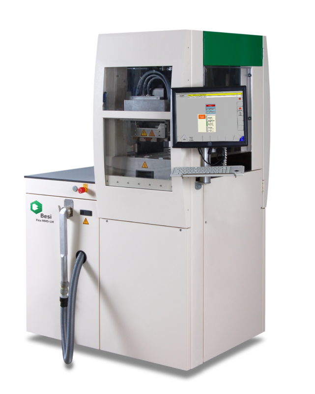
Thermal analysis
Filtronic can provide full thermal analysis which is critical in selecting the correct die attach material, interconnect, and mould compound for the package design. Our expertise covers CTE mismatch and voiding.
Our end-end process includes a range of die-attach materials and interposers.
Capability to support volume production with full traceability of wafer and assembly lots.
Downloads


Featured products
Taurus
81-86GHz
In terms of performance, our high power amplifier redefines E-band power for commercial and military applications.
Find out more
Morpheus II
70-90GHz
Morpheus II modules are designed for easy incorporation into ODUs for rapid time to market with minimal customer engineering resource. They are a drop-in mmWave solution for ultra-high-capacity wireless links.
Find out more
Related media
Popular news, articles and white papers
- Pushing the boundaries in LEO applications – Filtronic expands presence in satellite communications market
- Filtronic launches into the future, securing a Strategic Partnership with SpaceX for Starlink constellation
- Filtronic secures further order, strengthening strategic partnership with SpaceX for Starlink
- Filtronic cements position in LEO market with a new follow-on contract for Cerus 32
- Filtronic & Marubun Corporation sign MoU to strengthen Japan’s communications resilience
- Filtronic Unveils Advanced High Bandwidth DIFI Solution to Enable Fully Virtualised Satellite Ground Stations
- Filtronic awarded £4.5 million contract with BAE Systems
- Filtronic opens new Headquarters & Manufacturing Facility
- Filtronic wins a new radar contract from Defence Prime
- Filtronic Secures key role in European Defence Sector Programme
- Filtronic awarded NSIP funding to develop next-generation 550W Ka-Band SSPA
- Filtronic Secures Record Breaking SpaceX Order
- Filtronic secures $9 Million order to boost SpaceX’s Starlink deployment with advanced E-band SSPAs
- Filtronic completes multi-year GaN packaging project
- A transformative year for Filtronic
- Filtronic releases highest power (>20W), commercially available E-band solid-state power amplifier (SSPA) on the market
- Filtronic strengthens its position within the E-band low Earth orbit market with second-generation Cerus 32 power module
- Unveiling the future of E-band
- Filtronic bolsters global commercial team with two senior appointments
- Filtronic ushers in new leadership era with CEO Nat Edington