GaN design and manufacturing challenges for phased array applications
GaN design and manufacturing challenges for phased array applications
Jerry Sanham, Business Development Director, Filtronic
Originally printed in Microwave product digest May 2021
High-power gallium nitride (GaN) devices are becoming increasingly prevalent in the transmit chain of phased array antennas, not only for radar but more recently also for 5G active antennas. GaN’s high breakdown voltage and high power density, combined with its good thermal conductivity, have made it the technology of choice for power amplification in phased array antenna designs where size, reliability and efficiency are the prime considerations. This article explores the challenges in producing GaN-based products for these applications and discusses assembly techniques for improving yield and performance.
Why GaN for phased arrays?
Modern phased array radars can incorporate more than 10,000 elements, with the gain of the overall antenna structure being a function of the number of elements as well as the gain of each element. With element spacing fixed by electrical design constraints at around half a wavelength [1], packing this many elements into a defined space outline inevitably generates a large amount of heat, and this must be safely dissipated without affecting performance and reliability.
Massive MIMO (mMIMO) antennas for 5G base stations—currently with up to 64 transmit and 64 receive elements—are smaller, but power consumption and weight are major considerations. Already tower companies are becoming concerned about the weight of these active array antennas requiring a large crane for installation, and for tower construction to be reinforced.
Although still sometimes considered a ‘new technology’ GaN has already been used extensively for both military and commercial applications, and yet still has considerable potential to extend into the mmWave region.
Wolfspeed [2] has summarized the advantages of GaN as follows:
- GaN can achieve much higher power levels for a specific die size, due to its higher power density
- GaN-on-SiC has demonstrated reliability at higher junction temperatures than other technologies, and also has superior thermal handling capability due to the high thermal conductivity of SiC
- Due to having a wide bandgap, GaN can operate at wider bandwidths, as its smaller size for a given power level reduces output impedance and makes wideband matching easier
- The higher power density and optimal output impedance of GaN also allow it to achieve better efficiencies at higher power levels, which is particularly important in a phased array where multiple PA modules are densely packed.
Further to this last point, Qorvo [3] has quantified the thermal advantage of GaN over GaAs. For a one-million-hour median time to failure (MTTF), a GaN device can comfortably operate at a channel temperature 50°C higher than GaAs. All of these considerations mean that GaN is now the preferred technology for power amplification in phased array T/R modules.
Design challenges
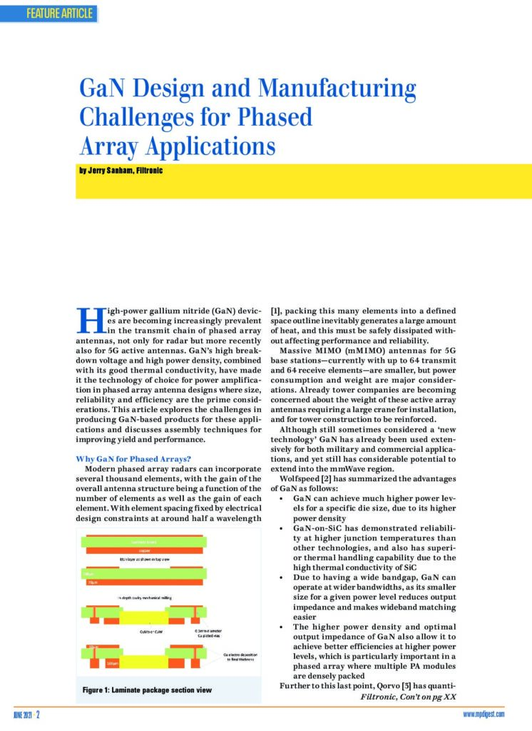
In addition to the normal constraints of microwave design, the additional challenges in designing high-power, densely-packed transmit/receive (T/R) modules for phased arrays are both mechanical and thermal. Any type of packaging will have an impact on both performance and thermal impedance, and therefore reliability. One approach for the high power and dependability demanded by phased array systems is to integrate bare die into modules using surface-mount laminate as subsystem-level packaging, as shown in Figure 1. The commercial laminate material used for packaging can often be the same or similar to that of the PCB, thereby providing a good thermal match. Figure 2(a) and (b) show in more detail the features of the package.
Care is required to ensure that the thermal conductivity of the die attach is as high as possible, to dissipate heat and minimize the junction temperature. The material to which the die is bonded also needs to be closely matched in coefficient of thermal expansion (CTE) to avoid placing unnecessary strain on the chip and potentially causing damage to the die bond.
In the RF design phase, state-of-the art microwave design tools including 3D electromagnetic modeling, along with AWR Microwave Office and Keysight ADS, ensure sound electrical performance to meet demanding specifications, including maximizing power added efficiency to keep the junction temperature as low as possible for a given power level. Thermal simulation software is also used to optimize the dissipation of generated heat.
Direct integration of bare GaN die into microwave assemblies under cleanroom conditions requires in-house automatic die attach and wire bond capability. Vacuum picking from waffle packs or reels and fully-automated placement equipment (Figure 3) enables tightly controlled, accurate and repeatable die placement with X/Y accuracy of ±10µm. The accuracy of bare die placement directly impacts the bond wire length, which in turn may impact RF performance especially at mmWave frequencies. Using a bare die technique ensures that the highest level of performance is achieved without the need for the additional complexity of packaging. Hybrid construction methods offer the ability to mix and match technologies, and to include other components like quartz filters and printed microstrip components as well as packaged SMT passive components.
Addressing thermal challenges
It is critical for reliability that die-attach should be optimized to keep die temperature, and thus channel temperature, to a minimum. Three common methods of die attach are available—epoxy, eutectic, and pressure-less silver sintering. High conductivity epoxy typically has a thermal conductivity (k) value of up to 60W/mK, while gold-tin (AuSn) eutectic solder has a k value of approximately 57W/mK. Both of these methods have been used for attaching GaN die, but superior thermal performance can be obtained by using pressure-less silver sintering, which has a higher k in excess of 200W/mK.
The design of the module packaging is also crucial, and a solid copper paddle will disperse the heat as rapidly as possible, as shown in Figure 2(b). This provides a good thermal conductivity of typically 401W/mK, and eliminates ground via inductance since there are no vias in the ground paddle itself.
The challenge is that the high differential between the CTE of the SiC substrate of the GaN chip and that of copper potentially causing delamination under temperature cycling. Mounting the die onto copper molybdenum (CuMo) or copper tungsten (CuW) alloy improves the die-to-package CTE match. If epoxy die bonding is used, then a thicker epoxy layer can absorb some of the mismatch, but unfortunately at the expense of reducing the thermal conductivity of the bond.
It is often the case that a newly-assembled module will exhibit extremely good die shear performance, exceeding specification by an order of magnitude. When this is put through 1,000 temperature cycles, however, it can degrade to the extent that it will fail the die shear test. Considerable work has taken place on optimizing the die attach technology to prevent such failures, and test pieces are put through cycling to ensure this.
Minimizing voiding
Voiding—areas where the die is not attached—is one of the key reliability metrics for a GaN PA. MIL-STD-883 J TM 2012.9 specifies that the area of voiding underneath the die must not exceed 10% of the die area. Producing batches of between 5,000 and 10,000 high-power GaN amplifiers, Filtronic is currently achieving yields of 97% against the void specification.
With 2,500 square feet of Class 100,000 clean rooms at its UK hybrid microelectronics assembly facility, Filtronic has the capability to assemble microwave and mmWave devices into surface mountable (SMT) modules, in the form of system-in-package (SIP) and multi-chip modules (MCM). The microwave and mmWave devices could include chip scale ball grid arrays (BGA) and flip chip die.
In addition to low-void die attach and precision component placement, Filtronic’s assembly and test capability includes fully-automated wire and ribbon bonding with deep-access multi-level capability, sub-assembly manufacturing, skilled manual assembly, hermetic sealing, and automated test to 90GHz. MIL-STD-883 processes and procedures are supported by Six Sigma, along with high levels of production automation and strict traceability. As well as optimizing die-attach and heat-sinking for power devices, particular attention is also focused on minimizing wire-bond parasitics for products that operate at higher frequencies. Reliability and tolerance to harsh environments are evaluated in-house using high-temperature operating life (HTOL) testing, highly accelerated stress test (HAST) and humidity testing.
To date, over 60,000 T/R modules for phased array radar have been successfully shipped, at production rates in excess of 3,500 per month
References
[1] Microwaves 101 Encyclopedia, https://www.microwaves101.com/encyclopedias/phased-array-antennas
[2] ‘GaN MMICs for mmWave applications’, Jeremy Fisher, Wolfspeed, at 2019 Interlligent RF and Microwave Seminar https://youtu.be/xiGCylz6_aw [3] ‘RF Applications of GaN for Dummies’, Qorvo eBook, https://www.qorvo.com/design-hub/ebooks/gan-for-dummies